


The answer, in actual fact, is that Nikon can beat Sony at their own game, with the 46MP full frame sensor in the D850 proof of the pudding. It does better 4K video quality than the A7R III at a higher megapixel count and edges it for stills quality too. Now let’s hear about some of the science behind it.
First head over to Imaging Resource and read the full post there, a masterpiece of an article that will extend anyone’s understanding of camera sensors to an extremely high level.
Nikon operate within the modern limits of manufacturing capabilities, at the foundries they use for chip manufacture (including Sony’s). However, a large in-house design team lays out custom sensors in microscopic detail, right down to determining the size and shape of everything from transistors and photodiodes to microlenses and readout circuitry, according to Dave’s article.
They then simulate not just the complete chip circuitry but the manufacturing process down to the individual atomic level at nanosecond intervals.
Nikon also develop their own custom sensor readout, so that they can design the entire image pipeline in parallel with the Expeed image processor. In the case of the D850 this leads to a digital low pass filter to reduce moire in full frame 4K, which has to be pixel binned from the full 46MP resolution…basically 8K. Their own sensor design also allows low sensitives such as true ISO 64, which Sony is yet to offer.
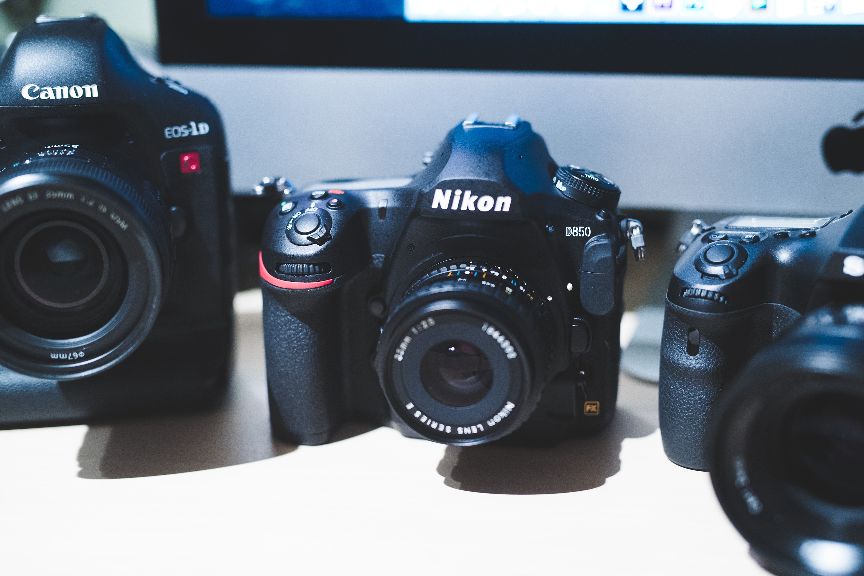
D850 and D5
Nikon have developed themselves every aspect of the D5 and D850 sensors, including the microlenses which focus light as efficiently as possible into the photodiodes. In designing their own micro lenses they can optimize the sensor for F-mount lenses.
The job of the photodiode is to convert photons into analogue electrical voltages, which are then converted from analogue to digital signals by a column A/D converter.
This is key to achieving 4K video, because with such a lot of resolution being converted from analogue voltages to digital 1s and 0s at 24 frames per second, you need a LOT of A/D converters. These have been reduced to such a small scale that they sit on the edge of the sensor itself at every column and operate in tandem.
There’s so much data in the pipeline at this point that Nikon has to encode the signal to ensure it is transmitted error-free and under the speed limits of the chip.
Nikon has a separate team of experts for each camera sensor. They can prototype sensor designs in software, with what Dave describes as “an entire semiconductor factory in the CAD software, with the computer simulating every step of the fabrication process down to an atomic level”.
It’s REALLY important for Nikon that they have correlation between this software and the real thing, so that their design stands up when it comes to actual manufacturing. It’s a bit like the windtunnel at a Formula One car team – you can’t design a good wing unless that tunnel perfectly simulates how it behaves on track.
What Dave reveals about this part of the design process at Nikon is mindblowing:
“It’s hard to convey just how insanely detailed the CAD simulations of the semiconductor processing are. One minor example: To make semiconductor devices, you introduce tiny amounts of impurities into the silicon, to change its electrical properties. These days, this is done by using room-sized particle accelerators to smash impurity atoms into the silicon at very high energies. In sensor manufacturing, it’s not uncommon for these “ion implanters” to operate at energies of a million volts or more(!). But a lot can happen on the way from the accelerator into the silicon, so the simulation software traces the paths of individual impurity atoms, as they smash through the photoresist, refract through the edges of it, and reflect off other structures”
Even with a simulation of this ambition and fine granularity, it is backed up by actual silicon prototyping, with test circuits implanted in real wafers, fabricated like a final production sensor. It’s a prototyping stage which takes a lot of investment in R&D.
You can be sure that if Nikon makes their own sensors for the upcoming FX Z-mount mirrorless cameras, they will be true Nikon custom silicon and not just a “greatest hits” of other people’s technology. Indeed it might not even matter if they are manufactured in facilities owned by Sony, Toshiba or TowerJazz – it is the design process which is key to defining the performance, both for stills and video.